
Introduction
Semiconductor materials used in power electronics are transitioning from silicon to wide bandgap semiconductors such as silicon carbide (SiC) and gallium nitride (GaN) due to their superior performance in automotive and industrial applications. GaN and SiC enable smaller, faster and more efficient designs. Regulatory and economic pressures continue to push efficiency gains in high-voltage power electronics designs. The power-density advantages of smaller and lighter designs are particularly evident in space-constrained and/or mobile usages such as electric vehicles, but compact power electronics are more broadly desirable as well, especially from the standpoint of reduced system cost. At the same time, efficiency is growing in importance as governments introduce financial incentives and more stringent energy-efficiency regulations.
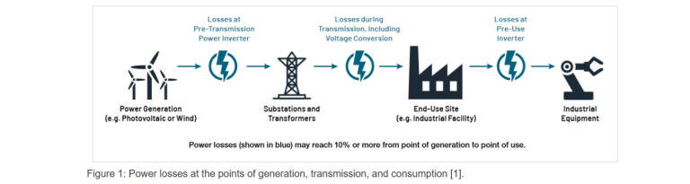
Guidelines issued by global entities, such as the European Union’s Eco-design Directive, the United States Department of Energy 2016 Efficiency Standards, and China’s Quality Certification Centre (CQC) Mark govern energy efficiency requirements for electrical products and equipment. The need to enact greater energy efficiency in power electronics stretches from the point of power generation to the point of consumption, as illustrated in Figure 1. Power converters operate at multiple stages throughout the generation, transmission, and consumption chain, and, because none of those operations is 100% efficient, some power loss occurs at each step. Chiefly due to energy lost as heat, these reductions in overall efficiency multiply throughout the cycle. [1]
When designing power converters, a 0% power loss is ideal as illustrated in Figure 2.
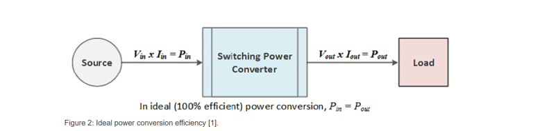
A typical converter would have an efficiency of about 87% to 90%, meaning that 10% to 13% of the input power is dissipated within the converter, mostly as waste heat. A significant portion of this loss is dissipated in the switching devices such as MOSFETs or IGBTs. [2]
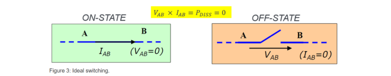
Ideally, the switching device is either “on” or “off” as shown in Figure 3 and instantaneously switches between these states. In the “on” state, the impedance of the switch is zero ohms and no power is dissipated in the switch, regardless of how much current is flowing through it. In the “off” state, the impedance of the switch is infinite, and zero current is flowing, so no power is dissipated.
In practice, power is dissipated during the transition between “on” and “off” (turn-off) and between “off” and “on” (turn-on). These non-ideal behaviors occur because of parasitic elements in the circuit. As shown in Figure 4, the parasitic capacitances on the gate slow down the switching speed of the device, extending the turn-on and turn-off times. The parasitic resistances between the MOSFET drain and source dissipate power whenever drain current is flowing. [2]

There’s also reverse recovery loss of the body diode in the MOSFET to consider. Reverse recovery time of the diode is a measure of the switching speed in the diode and thus affects the switching losses in the converter design.
Therefore, design engineers will need to measure all these timing parameters in order to keep the switching losses at minimum and thus design more efficient converters.
The preferred test method to measure the switching parameters of MOSFETs or IGBTs is the “Double Pulse Test” method. This application note will describe the Double Pulse Test and how it’s implemented. In particular, this application note will explain how to generate pulses with the Tektronix AFG31000 Arbitrary Function Generator and measure important parameters with a 4, 5 or 6 Series MSO oscilloscope.